
Author Affiliations
Abstract
1 School of Science and Engineering and Shenzhen Key Laboratory of Semiconductor Lasers, The Chinese University of Hong Kong, Shenzhen (CUHKSZ), Shenzhen 518172, China
2 Department of Electronic and Electrical Engineering, University College London, London WC1E 7JE, UK
3 Université Grenoble Alpes, CNRS, CEA-LETI, MINATEC, LTM, F-38054 Grenoble, France
Monolithic integration of III-V lasers with small footprint, good coherence, and low power consumption based on a CMOS-compatible Si substrate have been known as an efficient route towards high-density optical interconnects in the photonic integrated circuits. However, the material dissimilarities between Si and III-V materials limit the performance of monolithic microlasers. Here, under the pumping condition of a continuous-wave 632.8 nm He–Ne gas laser at room temperature, we achieved an InAs/GaAs quantum dot photonic crystal bandedge laser, which is directly grown on an on-axis Si (001) substrate, which provides a feasible route towards a low-cost and large-scale integration method for light sources on the Si platform.
lasers bandedge photonic crystal monolithic integration quantum dots silicon substrate Chinese Optics Letters
2022, 20(4): 041401

Author Affiliations
Abstract
1 Department of Electronic and Electrical Engineering, University College London, Torrington Place, London, WC1E 7JE, United Kingdom
2 Institute of Photonic Integration, Eindhoven University of Technology, Eindhoven 5600 MB, The Netherlands
3 QD Laser, Inc., Kawasaki 210-0855, Japan
4 Centre for Photonics Systems, Department of Engineering, University of Cambridge, Cambridge CB3 0FA, United Kingdom
5 e-mail: z.cao@tue.nl
Semiconductor mode-locked lasers (MLLs) are promising frequency comb sources for dense wavelength-division-multiplexing (DWDM) data communications. Practical data communication requires a frequency-stable comb source in a temperature-varying environment and a minimum tone spacing of 25 GHz to support high-speed DWDM transmissions. To the best of our knowledge, however, to date, there have been no demonstrations of comb sources that simultaneously offer a high repetition rate and stable mode spacing over an ultrawide temperature range. Here, we report a frequency comb source based on a quantum dot (QD) MLL that generates a frequency comb with stable mode spacing over an ultrabroad temperature range of 20–120°C. The two-section passively mode-locked InAs QD MLL comb source produces an ultra-stable fundamental repetition rate of 25.5 GHz (corresponding to a 25.5 GHz spacing between adjacent tones in the frequency domain) with a variation of 0.07 GHz in the tone spacing over the tested temperature range. By keeping the saturable absorber reversely biased at , stable mode-locking over the whole temperature range can be achieved by tuning the current of the gain section only, providing easy control of the device. At an elevated temperature of 100°C, the device shows a 6 dB comb bandwidth of 4.81 nm and 31 tones with optical signal-to-noise ratio. The corresponding relative intensity noise, averaged between 0.5 GHz and 10 GHz, is . Our results show the viability of the InAs QD MLLs as ultra-stable, uncooled frequency comb sources for low-cost, large-bandwidth, and low-energy-consumption optical data communications.
Photonics Research
2020, 8(12): 12001937
Author Affiliations
Abstract
Department of Electronic and Electrical Engineering, University College London, London WC1E 7JE, UK
In the past few decades, numerous high-performance silicon (Si) photonic devices have been demonstrated. Si, as a photonic platform, has received renewed interest in recent years. Efficient Si-based III–V quantum-dot (QDs) lasers have long been a goal for semiconductor scientists because of the incomparable optical properties of III–V compounds. Although the material dissimilarity between III–V material and Si hindered the development of monolithic integrations for over 30 years, considerable breakthroughs happened in the 2000s. In this paper, we review recent progress in the epitaxial growth of various III–V QD lasers on both offcut Si substrate and on-axis Si (001) substrate. In addition, the fundamental challenges in monolithic growth will be explained together with the superior characteristics of QDs.
Journal of Semiconductors
2019, 40(10): 101302

Author Affiliations
Abstract
Department of Electronic and Electrical Engineering, University College London, London, WC1E 7JE, United Kingdom
Over the past decades, the progress in the growth of materials which can be applied to cutting-edge technologies in the field of electronics, optoelectronics and energy harvesting has been remarkable. Among the various materials, group III–V semiconductors are of particular interest and have been widely investigated due to their excellent optical properties and high carrier mobility. However, the integration of III–V structures as light sources and numerous other optical components on Si, which is the foundation for most optoelectronic and electronic integrated circuits, has been hindered by the large lattice mismatch between these compounds. This mismatch results in substantial amounts of strain and degradation of the performance of the devices. Nanowires (NWs) are unique nanostructures that induce elastic strain relaxation, allowing for the monolithic integration of III–V semiconductors on the cheap and mature Si platform. A technique that ensures flexibility and freedom in the design of NW structures is the growth of ternary III–V NWs, which offer a tuneable frame of optical characteristics, merely by adjusting their nominal composition. In this review, we will focus on the recent progress in the growth of ternary III–V NWs on Si substrates. After analysing the growth mechanisms that are being employed and describing the effect of strain in the NW growth, we will thoroughly inspect the available literature and present the growth methods, characterization and optical measurements of each of the III–V ternary alloys that have been demonstrated. The different properties and special treatments required for each of these material platforms are also discussed. Moreover, we will present the results from the works on device fabrication, including lasers, solar cells, water splitting devices, photodetectors and FETs, where ternary III–V NWs were used as building blocks. Through the current paper, we exhibit the up-to-date state in this field of research and summarize the important accomplishments of the past few years.
Journal of Semiconductors
2019, 40(10): 101301
Author Affiliations
Abstract
1 Department of Electronic and Electrical Engineering, University College London, London WC1E 7JE, UK
2 State Key Laboratory of Optoelectronic Materials and Technologies, Sun Yat-sen University, Guangzhou 510275, China
3 Department of Physics and Astronomy, Cardiff University, Cardiff CF24 3AA, UK
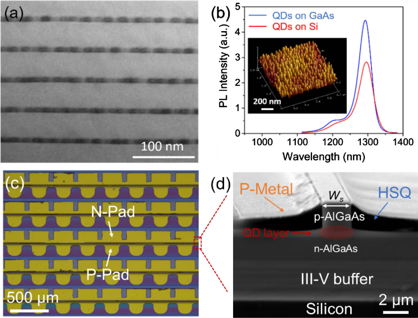
We report low-noise, high-performance single transverse mode 1.3 μm InAs/GaAs quantum dot lasers monolithically grown on silicon (Si) using molecular beam epitaxy. The fabricated narrow-ridge-waveguide Fabry–Perot (FP) lasers have achieved a room-temperature continuous-wave (CW) threshold current of 12.5 mA and high CW temperature tolerance up to 90°C. An ultra-low relative intensity noise of less than 150 dB/Hz is measured in the 4–16 GHz range. Using this low-noise Si-based laser, we then demonstrate 25.6 Gb/s data transmission over 13.5 km SMF-28. These low-cost FP laser devices are promising candidates to provide cost-effective solutions for use in uncooled Si photonics transmitters in inter/hyper data centers and metropolitan data links.
Photonics Research
2018, 6(11): 11001062

Author Affiliations
Abstract
1 State Key Laboratory of Information Photonics and Optical Communications, Beijing University of Posts and Telecommunications, Beijing 100876, China
2 State Key Laboratory of Alternate Electrical Power System with Renewable Energy Sources, North China Electric Power University, Beijing 102206, China
3 Laboratory of Nano Optoelectronics, Institute of Semiconductors, Chinese Academy of Sciences, Beijing 100083, China
4 Engineering Research Center for Semiconductor Integrated Technology, Institute of Semiconductors, Chinese Academy of Sciences, Beijing 100083, China
5 Department of Electronic & Electrical Engineering, University College London, London WC1E 7JE, UK
We report on the first electrically pumped continuous-wave (CW) InAs/GaAs quantum dot (QD) laser grown on Si with a GaInP upper cladding layer. A QD laser structure with a Ga0.51In0.49P upper cladding layer and an Al0.53Ga0.47As lower cladding layer was directly grown on Si by metal–organic chemical vapor deposition. It demonstrates the postgrowth annealing effect on the QDs was relieved enough with the GaInP upper cladding layer grown at a low temperature of 550°C. Broad-stripe edge-emitting lasers with 2-mm cavity length and 15-μm stripe width were fabricated and characterized. Under CW operation, room-temperature lasing at ~1.3 μm has been achieved with a threshold density of 737 A/cm2 and a single-facet output power of 21.8 mW.
Quantum-well, -wire and -dot devices Semiconductor lasers Integrated optics materials Photonics Research
2018, 6(4): 04000321


